Key information:
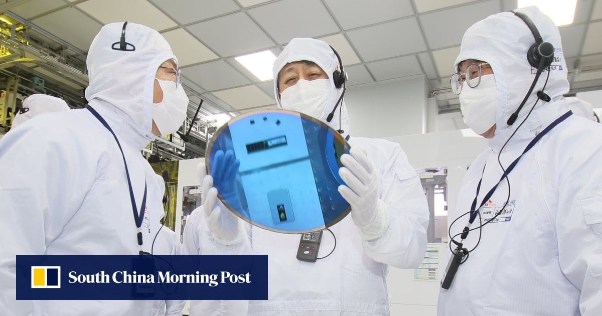
South Korea will spend the money to build 13 new chip plants and three research facilities, on top of an existing 21 fabs. Spanning Pyeongtaek to Yongin, the area is expected to be the largest in the world, capable of producing 7.7 million wafers monthly by 2030.
As part of the two-decade plan, Samsung and Hynix are set to build their most sophisticated chip plants at home. Samsung’s betting big on foundry – or making chips for other firms – as part of a 500 trillion won investment by 2047. Smaller rival Hynix aims to invest 122 trillion won in memory in Yongin over the same period.
The government said the region will also house smaller chip design and materials companies. The overarching ambition is to improve the country’s self-sufficiency in semiconductors, while increasing its market share of global logic chip production to 10 per cent by 2030 from 3 per cent now.
?Pangyo, where fabless firms are now concentrated, will be the hub of low-powered, high-performance AI chips. Suwon will be a central test bed for compound semiconductors, while Pyeongtaek will see a new semiconductor R&D centre at Korea Advanced Institute of Science and Technology’s new campus to be completed by 2029.


