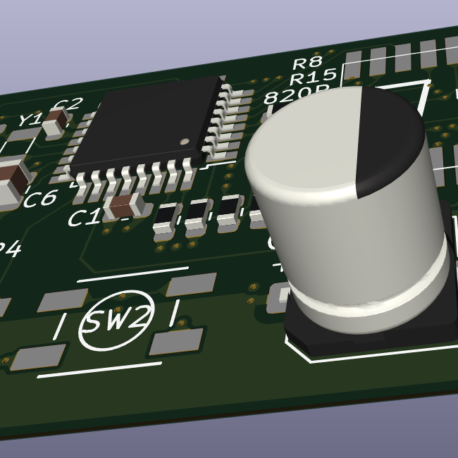
Hello everyone, I need some advice.
I am making custom PCBs for a project of mine. It’s basically for a little remotely controlled robot using little DC motors. I chose the Seeed Studio XIAO ESP32C3 as the uC since it has inbuilt wifi/bt, 3.3V regulator that I can use to power the motors (can source up to 700mA) and lipo charging management (the robots will run on battery). As you can see from here, the microcontroller is surface mounted and the pads for the battery are on the bottom layer. Same story goes for the thermal pad of the microcontroller and the thermal pad of the motor driver (datasheet). I have worked with SMD components in the past and can solder them by hand, but I have never worked with SMD components that have thermal pads on the bottom layer. My question is: how to manage (route?) them? My PCB is 2-layer and I was planning on having both layers filled with a ground plane. Do I just connect thermal pads to the ground plane and call it a day? Wouldn’t that make the components hard to solder with hot air? Do I make an isolated polygon that only acts as a thermal pad?
Speaking of soldering is even hot air the way to go in this case? My PCB has components on both sides, and I was planning on ordering stencils together with the boards and using solder paste, placing the components and then using hot air to solder the components in place. I thought a hot plate would be better but I don’t have access to one and I don’t know how that works with components on both sides.
I attached some photos of the PCB in Kicad, and here’s the git repo. If it is of any help, I’m planning of having them manifactured by JLCPCB. It is also my first time using KiCad, so go easy on me :)
Thanks!


I usually try and go a bit higher for trace size than needed to avoid complication and aid in heat dissipation. My signals are by default .25 and my power traces are usually between .5 and .75 (my teacher argues for 1 and 1.5).
There are trace width calculators online like on digikey that can tell you he minimum you need.
Your vias are fine though, I usually go 0.5/0.3 . If you bring up your power traces, you have to keep in mind a vias hole should be the same size or bigger than the trace.
I also edited my other comment while you were replying, sorry.